1. Characteristics of photoresist porcelain
After the photoconductive material is added with an electrode, it forms a photoresist. When studying the formula and process of photoresist, we must first understand the characteristics of photoresist. Photoresist porcelain has the following characteristics:
(1) Spectral characteristics
This refers to the wavelength range of the light wave in which the photoresist sensitivity is the highest. For example, the peak sensitivity of CDs is 520nm and the peak sensitivity of CdSe is 720nm. When the two form a solid solution in different proportions, the peak sensitivity range changes continuously between 520 ~ 720nm.
(2) Sensitivity
Photoconductive sensitivity refers to the photocurrent generated under certain illumination conditions, which is related to the number of photogenerated carriers and the distance between electrodes. The representation methods are different in different applications.
The resistance value RD of photosensitive resistance without light is called dark resistance. The resistance value RP after illumination is called bright resistance.
Because the light resistance changes with the light intensity, the resistance sensitivity is meaningful only if it indicates what light intensity it is.
Dark resistance and bright resistance of photoresist can simply and clearly reflect the sensitivity of photoresist, so resistance parameters are also commonly used to represent the sensitivity of photoresist.
(3) Illuminance characteristics
The illuminance characteristic of photoresist refers to the characteristic that its output signal (voltage, current or resistance value) changes with the change of illuminance.
(4) Response time
The response time of photoresist is the rise time required for the bright current to reach a stable value under light and the attenuation time required for the bright current to disappear after shading. Usually 63.5% of the stable current is reached The required time of 2% is specified as the rise time, and 63.5% of the original stable current is attenuated after shading The time required for 2% is specified as the attenuation time. The response time varies with the irradiation light intensity. Response time and sensitivity are two contradictory parameters. If the response time is fast, the sensitivity is low. If the sensitivity is high, the response time becomes longer. Therefore, the manufacturing of photosensitive resistance should be comprehensively considered according to the application requirements.
(5) Temperature characteristics
The photoconductive and electrical properties of photoresist are greatly affected by temperature, and the relationship is complex. General temperature coefficient α T describes the temperature characteristics of the photoresist.
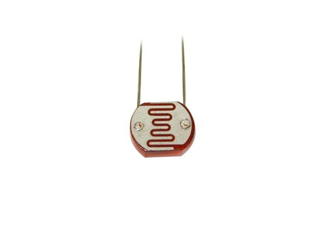
Fig Photosensitive resistance
2. Other photosensitive materials
(1) Preparation of photosensitive materials for electronic photography
Photosensitive materials for electronic photography require fine particles. Because the fine photosensitive powder can make the photosensitive layer uniform, and the contact area between particles increases, it can prevent overcurrent from burning the photoelectric device. There are many manufacturing methods of micro photoconductive powder, which can be summarized as follows. First, the existing photoconductive powder is further crushed to destroy its crystal and reduce the photoconductive sensitivity; The other is to burn the photoconductive powder with little or no flux in order to make the grain grow slowly. In the process of manufacturing photoconductive powder, the firing temperature should be lower than the melting point of flux to prevent excessive grain growth. However, these two methods can not achieve the purpose of photoconductive powder sensitization, and can not obtain photosensitive materials with high photoconductive sensitivity.
Another method is to add an appropriate amount of sensitizer and donor dopant into CDs powder, and then mix it to recrystallize CDs under high temperature and high pressure to obtain 5 μ High sensitivity photoconductive fine powder with particle size below M. However, this method requires a long time under high temperature and high pressure, so it is lack of practicability. A better method is to add dispersant to the ingredients when manufacturing photoconductive powder. During sintering, the dispersant can isolate the powder and obtain fine grains.
(2) Preparation of color TV camera tube target
An important application of photoconductive materials is to be used as targets in color TV camera tubes, and has been commercialized. Targets in color TV camera tubes include Sb2S3, PbO, Si, CdSe, etc.
Sb2S3 target - many targets with low photoelectric sensitivity and residual images on the fluorescent screen.
PbO target - complex manufacturing process, high cost and low sensitivity to red light.
Si target - because it is a single crystal chip, the image of the fluorescent screen is prone to white spots, and due to the use of integrated circuit technology, a matrix p-n junction is formed, resulting in poor image definition.
CdSe target - high photoconductive sensitivity, low dark current, and slight residual image will be temporarily left on the fluorescent screen.
Generally, the target of color TV camera tube is less sensitive to blue short wave light than green and red. The sensitivity of the whole color TV camera tube to light is determined by its sensitivity to blue. Therefore, as the target of color TV camera tube, it is required to be sensitive to all visible light, especially high sensitivity to blue light and fast transient response to light.